

wlcsp pkgWLCSP PKG
Ultra‑Compact, High‑Performance Packaging at Bare‑Die SizePACKAGE
WLCSP (Wafer‑Level Chip Size Package) is a chip‑size package in which the packaging process is completed at the wafer level.
Compared to conventional packages, WLCSP enables significant miniaturization and thickness reduction, making it ideal for products that require compact and lightweight designs, such as smartphones, wearable devices, and other small electronic devices.
LineupLINEUP
Oume Electronics proposes the optimal package structure based on your application and required specifications.
Cu Post Type
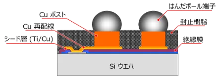
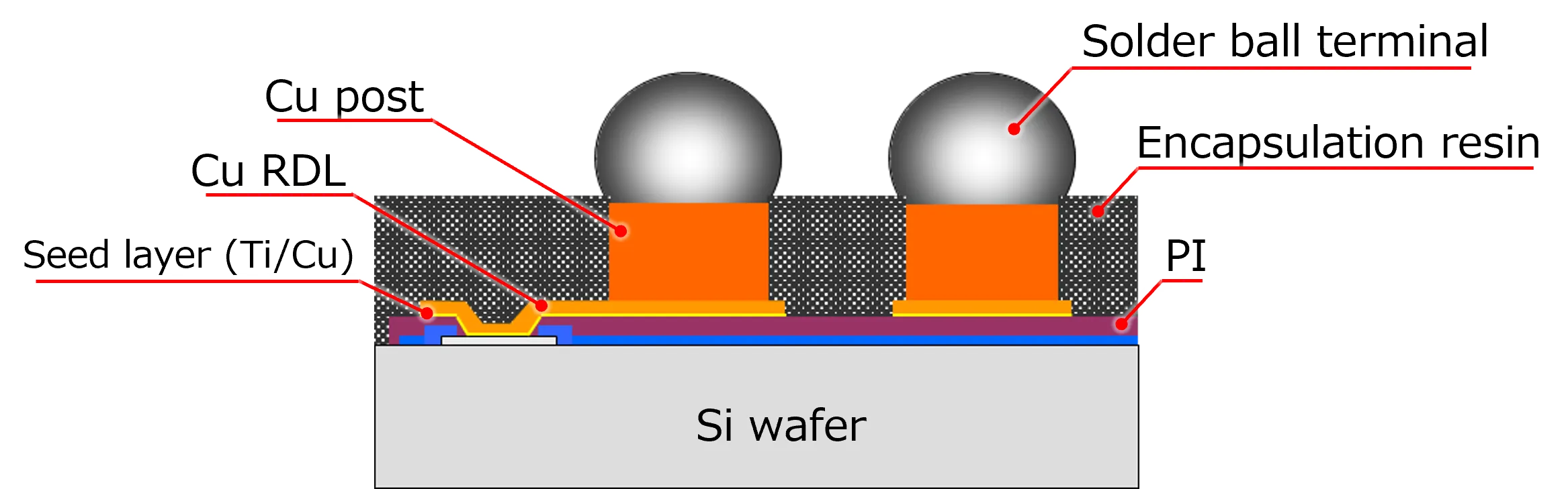
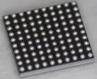
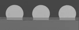
Features
- Highly reliable package
- Dielectric layer / Cu RDL / Cu post structure
- Epoxy resin encapsulation
- Chip‑size package identical to the original die dimensions
- Our unique package structure
Solder Materials
- Sn-Ag-Cu
- Note: For other terminal combinations, please contact us.
Supported Specifications
- Wafer sizes: 6, 8, 12 inch
- RDL Line/Space=min.10μm/min.10μm
- Bump pitch: Min.200μm
- Epoxy thickness: Typ.50μm
UBM Type
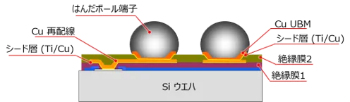
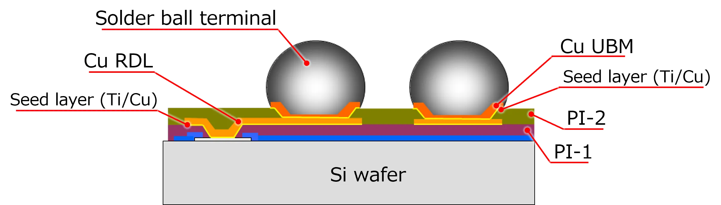

Features
- 2P2M structure
Solder Materials
- Sn-Ag-Cu
- Note: For other terminal combinations, please contact us.
Supported Specifications
- Wafer sizes: 6, 8 inch
- RDL Line/Space=min.10μm/min.10μm
- Bump pitch: Min.300μm
Reliability DataRELIABILITY
Oume Electronics’ WLCSP PKG has passed a range of rigorous reliability tests.
We provide stable and long‑term performance for various applications.
| Test Item | Conditions | Results | Remarks | |
|---|---|---|---|---|
| Cu POST | UBM | |||
| Reflow Resistance | 85℃、85%、168H | 10 | 10 | 260℃MAX 10sec |
| High‑Temp High‑Humidity Bias | 85℃、85%、3.5V/10V | 2000H | 1000H | (L/S : 10μm/10μm) |
| High‑Temperature Storage | 150℃ | 2000H | 1000H | |
| PCT | 121℃、100% | 500h | 168H | |
| Temperature Cycling | -65℃~+150℃ (30 min. each) | 1000cyc | 1000cyc | |
Application GuidelinesIMPLEMENTATION
We provide recommended conditions and precautions for mounting WLCSP onto boards.
