

bumping serviceBumping Service
Bump formation on customer‑supplied wafers for board‑embedded, module‑embedded, and flip‑chip applications.PROCESSING
LineupLINEUP
We propose the optimal bump structures according to your application and assembly method.
Solder‑Plated Bumps
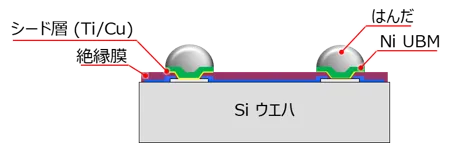
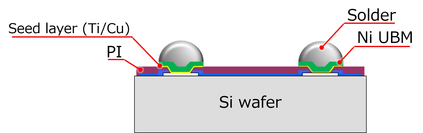
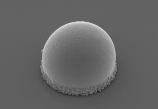

Features
- Solder bumps are formed on pads using a plating process
- Enables fine-pitch terminal formation
Bump Materials
- Ni/SnAg
Supported Specifications
- Wafer sizes: 6, 8, 12 inch
- Bump diameter: ≥ 12 µm
- Bump height: ≥ 10 µm
- Bump pitch: ≥ 27 µm
Applications
- C-MOS sensor
- Thermal Driver
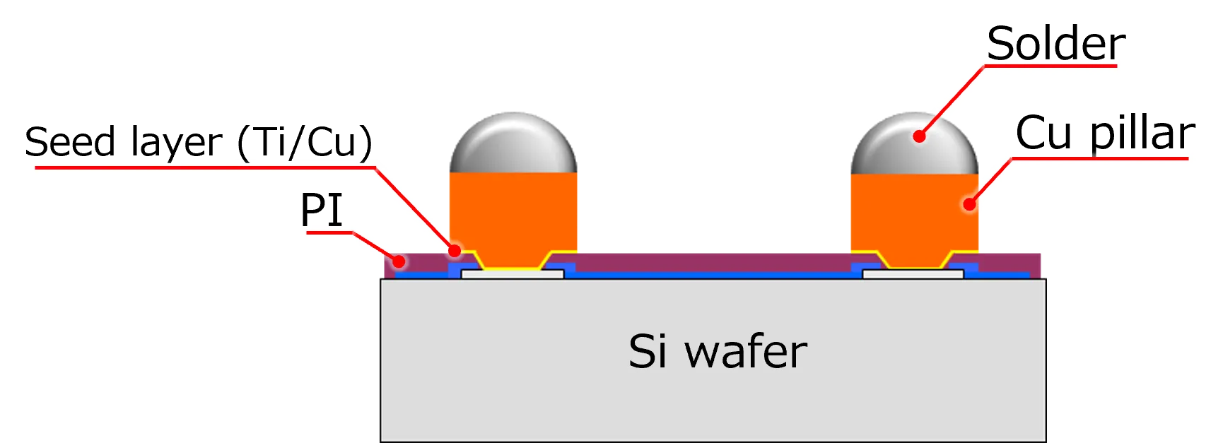
Cu Pillar
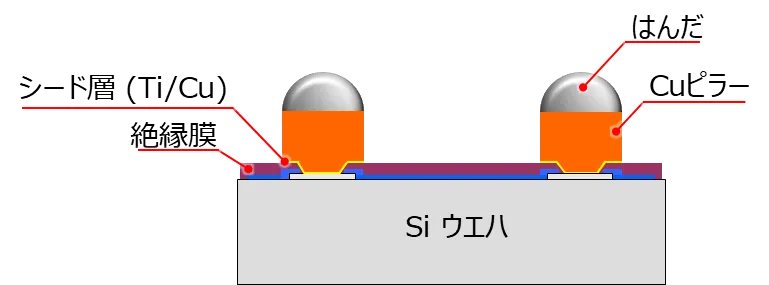
Features
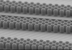
- Cu pillar and SnAg bumps are formed using a plating process
- Suitable for fine‑pitch applications
- Ideal for applications requiring clearance from the mounting substrate
Bump Materials
- Cu/(Ni)/SnAg
Supported Specifications
- Wafer sizes: 6, 8, 12 inch
- Pillar diameter: ≥ 12 µm
- Pillar height: approx. 13 µm to 80 µm
- Pillar pitch: ≥ 27 µm
- Cu pillar bumping can also be combined with RDL processing.
Applications
- DC/DC Converter
- Antenna SW
- e Fuse
- Optical Communication
- Mobile phone
- Wearable
- Battery
- Automotive
- MOS-FET
- 5G
- Base Stations
ApplicationsCASE
Oume Electronics’ bumping services are used across a wide range of applications.
Camera Image Sensors
Solder‑Plated Bumps
Thermal Print Head Drivers
Solder‑Plated Bumps
Aoi Electronics FOLP
Cu Pillar
Fine‑Pitch Cu Pillar
For FOLP® PSB
